
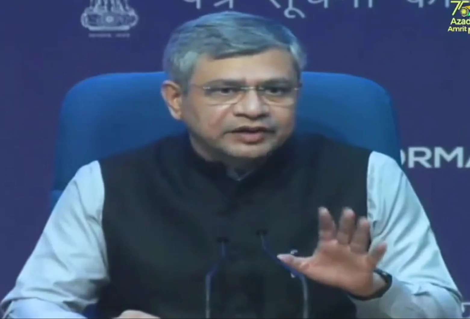
The government has approved a Rs 76,000-crore scheme to establish display and semiconductor industries in India, informed Ashwini Vaishnaw, Minister of Electronics and Information Technology (MeitY).
“Government of India is keen to incentivise and attract investment in setting up of Semiconductor FABs in India. This assumes significance in view of the fact that India is poised to increase its share in global manufacturing of Mobile Phones, IT Hardware, Automotive Electronics, Industrial Electronics, Medical Electronics, IoT and other devices in the near future as it aspires to have USD 400Bn of electronics manufacturing by the year 2025,” a government statement sadi.
Under this scheme, the government is offering financial support of up to 50 percent of the project cost to companies selected to set up semiconductor and display fabs. Support of up to 30 percent of capital expenditure will also be provided to set up semiconductor packaging facilities and compound semiconductors. The government expects at least 15 such units to be established. The scheme is also expected to generate 35,000 direct and 100,000 indirect jobs.
The government has divided the manufacturers into three categories.
- Category A: Is meant for the well established Integrated Device Manufacturers (IDMs) OR foundries OR Indian company / consortia with Indian industry partner. The requirement for this category includes having state-of-art mainstream CMOS technology nodes for fabricating processors, memories, analog / digital / mixed signal integrated circuits; or the company is desirous of setting up / expansion of existing Semiconductor FAB in India, preferably with a node size of 28nm or lower, wafer size of 300 mm and capacity of 30,000 WSPM or more.
- Category B: Again meant for well established Integrated Device Manufacturers (IDMs) or Foundries or Indian company / consortia with Indian industry partner, the company must have state-of-art compound semiconductor based emerging technologies for fabricating high frequency / high power / optoelectronics devices; or the company is desirous of setting up / expansion of existing Semiconductor FAB in India preferably with wafer size of 200 mm or more
- Category C: Under this, Indian companies / Consortia that are interested in the acquisition of Semiconductor FAB outside India
The last date for submitting EoI under this scheme has been extended till 30.04.2021.
Under a design linked incentive (DLI) scheme, the government plans to extend product design linked incentives of 50 percent of eligible expenditure; and product deployment linked incentives of 4-6 percent on net sales for five years.
“The vision of National Policy on Electronics 2019 (NPE 2019) is to position India as a global hub for Electronics System Design and Manufacturing (ESDM) and create an enabling environment for the industry to compete globally. One of the main strategies of NPE 2019 is to facilitate the setting up of Semiconductor FAB facilities and its ecosystem for design and fabrication of chips and chip components in India,” mentioned the statement.
- Amazon Warns Engineers Against AI Productivity Traps in Latest Memo
- Gnani AI Launches Prisma v3.0 Speech Recognition Model for 10 Languages
- Venttup Raises $3 Million To Expand Precision Manufacturing
- Articul8 Launches Bivia To Help Enterprise AI Agents Make Decisions
- NVIDIA Launches Open-Weight Transcription Model for 40 Languages
- Sarvam AI Rolls Out Indus Cowork to 2,500 Maharashtra Govt Officials