Scientists from Nanyang Technological University, Singapore, in collaboration with researchers from the Massachusetts Institute of Technology (MIT) in the US and the Skolkovo Institute of Science and Technology in Russia, have developed a machine learning approach that can predict changes to the properties of materials from straining the material.
This work could lead to the possibility of engineering new materials with tailored properties for potential use in communications, information processing, and energy fields, said a statement released by NTU.
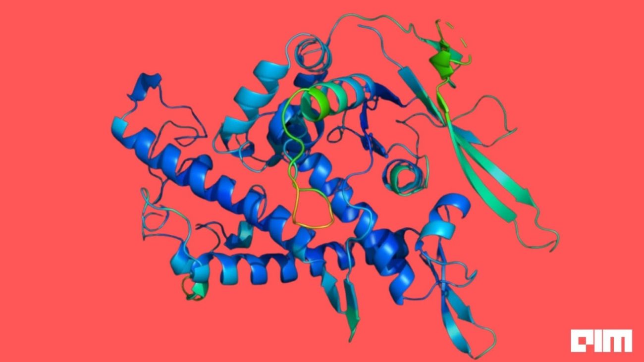
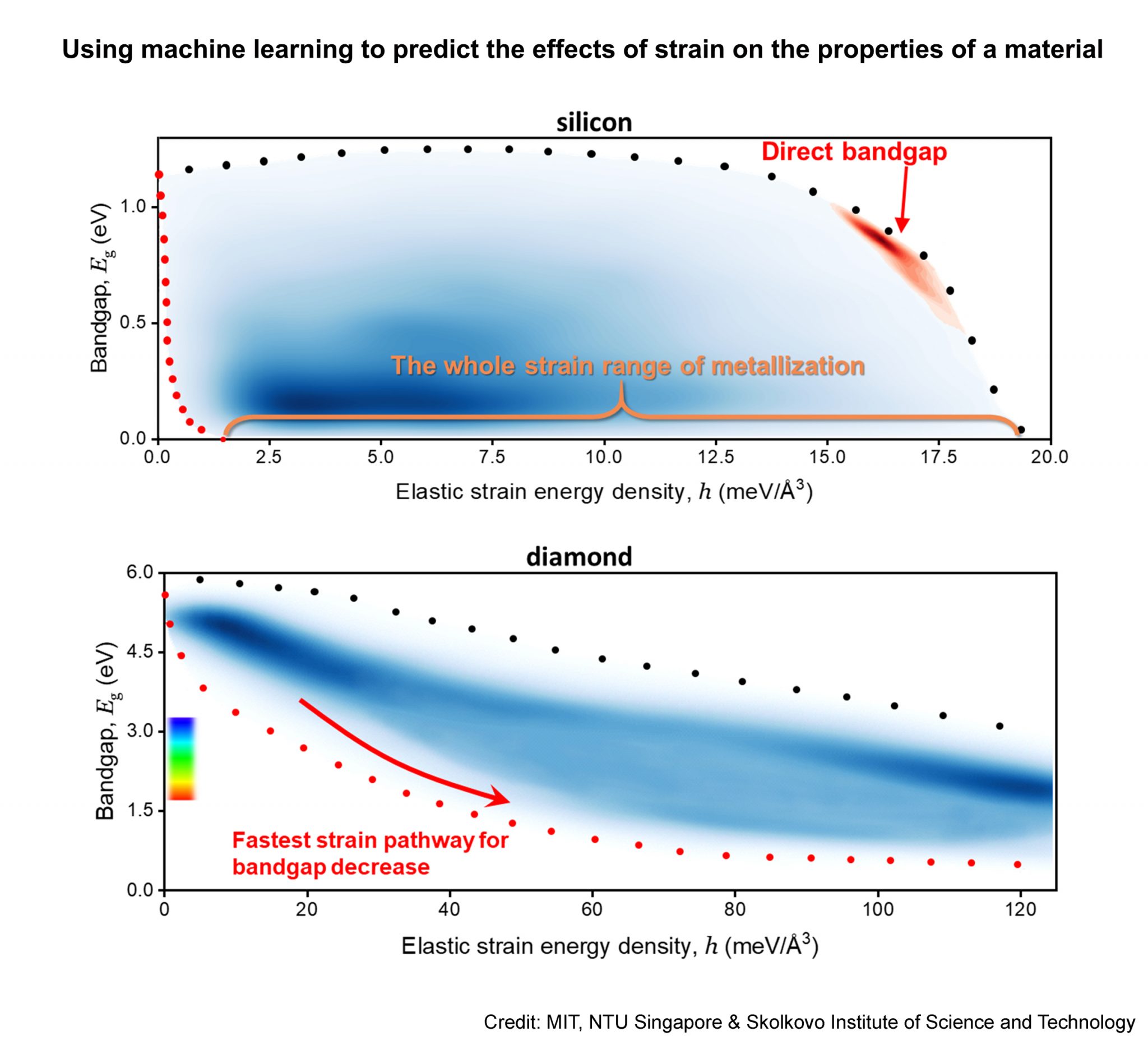
In a paper published earlier this week in the Proceedings of the National Academy of Sciences, the authors demonstrated their use of Artificial Intelligence to identify the most energy-efficient strain pathways that could transform diamond into more effective semiconductors.
When a semiconductor material is bent or strained, the atoms in its structure are perturbed, thus changing its properties such as how it conducts electricity, heat or the transmission of light. This process is known as ‘strain engineering’.
As a prelude to this work, last year the NTU Singapore and MIT authors reported in Science, that diamond nanoneedles could be bent and stretched as much as 9 per cent, which was surprising given that diamond is the hardest natural material known.
And in earlier research with industrial applications, “strain engineering” was used on silicon processor chips, where a one per cent strain allowed electrons to move faster, resulting in up to 50 per cent higher processing speeds.