
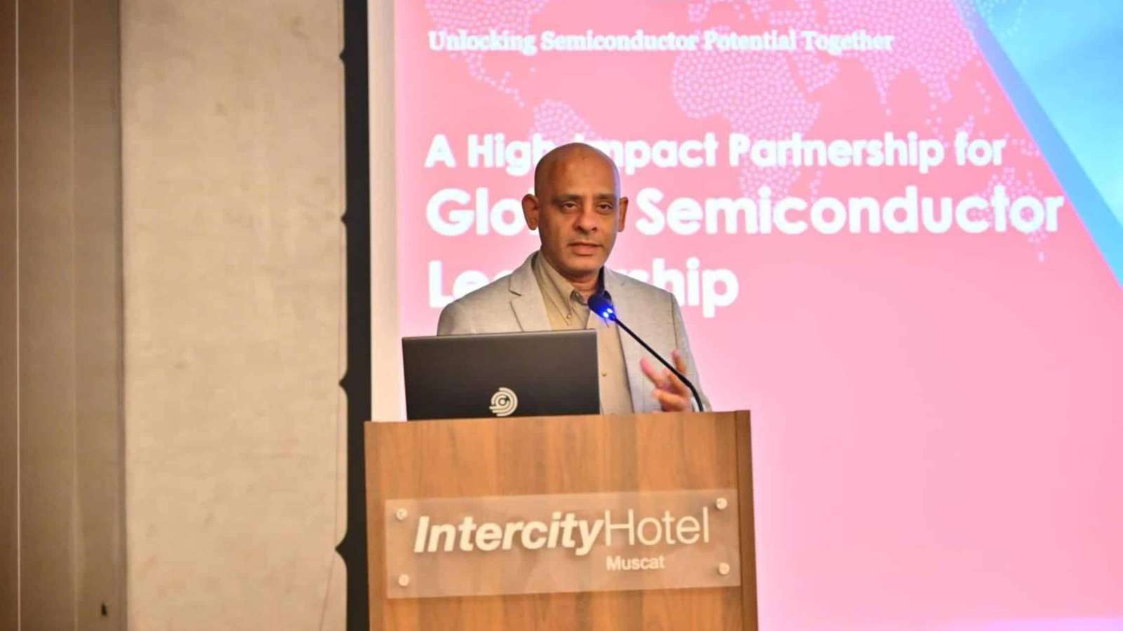
Kaynes Semicon, a subsidiary of Kaynes Technology, inaugurated its first international chip design centre in Muscat, Oman, on Sunday. The centre was established in collaboration with Oman’s Ministry of Transport, Communications and Information Technology (MTCIT), and the Ministry of Labour.
The new very large-scale integration (VLSI) design centre will focus on both front-end and back-end chip design processes. Raghu Panicker, CEO of Kaynes Semicon, stated, “The centre will help students with designing complex integrated circuits, chip fabrication, wafer preparation, etc.” The initiative aims to train 80 to 100 students annually in advanced VLSI design technologies.
The Omani government has fully funded the design centre. “With this step, we are extending our plan of building a strong semiconductor ecosystem beyond India, supporting local governments,” said Ramesh Kannan, managing director of Kaynes Technology India.
At the collaboration signing ceremony, Ali Al Shidhani, deputy minister of MTCIT, highlighted the importance of building a robust semiconductor sector as a critical pillar of the digital economy.
Kaynes Semicon is also progressing with plans to produce India’s first packaged semiconductor chip by July 2025. In September 2024, the company received approval from the Union Cabinet to set up an Outsourced Semiconductor Assembly and Test (OSAT) facility in Sanand, Gujarat, with an investment of ₹3,307 crore. The facility is expected to have a capacity to produce 6.3 million chips per day.
Kaynes Semicon’s move into Oman strengthens its research and development efforts and supports the growing semiconductor industry, helping both the company and Oman become rising players in global chip design and innovation. This initiative is integral to Oman’s National Program for Digital Economy and supports the vision of a diversified, knowledge-driven economy under Oman Vision 2040.
- AI Productivity to Add $28 Billion to $84 Billion to India's GDP: Cognizant Study
- OpenAI's Codex Helps in Aerodynamic Engineering for Mazda
- Bengaluru Accounts for 34% of India's FDE Talent: Report
- 84% See AI Productivity Gains, but Only 10% Allow Agent Autonomy: TCS Study
- Snowflake Introduces Business Ontology, Cortex AI Gateway to Bring AI Agents Into Enterprise Workflows
- Three Members Behind Claude Code Leave Anthropic Within 10 Days