Why Google Built Two TPUs Instead of One, and What it Signals for AI
By Smruthi Nadig ·
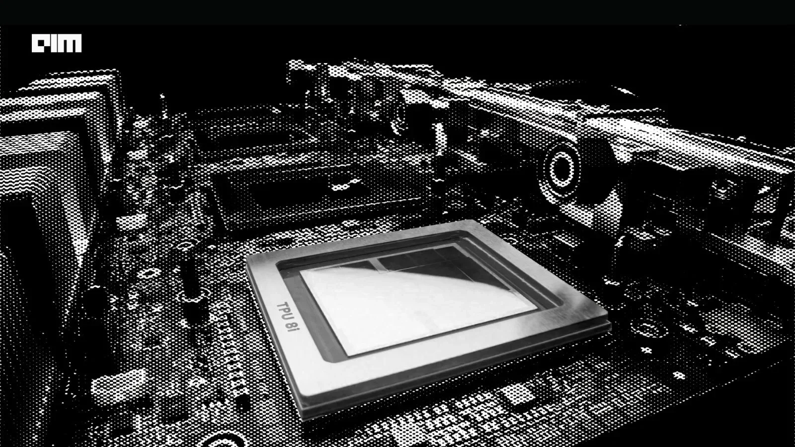
At its annual Cloud Next event, Google unveiled its eighth-generation tensor processing units (TPUs), marking a structural shift in how the company approaches AI infrastructure. For the first time, the company has introduced two distinct chips within the same generation—TPU 8t and TPU 8i—each purpose-built for different workloads in what it describes as the “agentic era.”
Google’s response is architectural specialisation. TPU 8t is designed for large-scale model training, while TPU 8i is engineered for inference and real-time reasoning workloads. Google has positioned the chips to address the scale, efficiency, and latency requirements associated with more complex AI systems.
Speaking to media, including AIM, Amin Vahdat, SVP and Chief Technologist of AI and Infrastructure at Google, frames this as part of a broader systems approach spanning energy, data centres, hardware, and software. “We don’t just insert at one layer of the stack… we get to go after the entire problem end-to-end,” he says.
As systems evolve from static models into agents capable of reasoning, planning, and executing multi-step tasks, infrastructure requirements are beginning to diverge. Training and inference, once treated as extensions of the same pipeline, are now being optimised separately.
Specialisation for Training and Inference
The introduction of TPU 8t and TPU 8i is based on a key realisation: the demands of training frontier models and serving them at scale are no longer identical.
TPU 8t, the training-focused chip, is built for compute-intensive workloads that require significant scale and throughput. A single TPU 8t superpod can scale up to 9,600 chips, delivering 121 exaflops of compute along with two petabytes of shared high-bandwidth memory. This architecture allows clusters to scale to very large sizes, reducing model training timelines.
Google notes the system also delivers up to 2.8x better price-performance compared with the previous generation, alongside improvements in storage access and data movement aimed at improving overall utilisation.
In contrast, TPU 8i is optimised for inference and reasoning, where latency, not throughput, is the primary constraint. Agentic workloads, which involve multiple interacting models operating in real time, tend to amplify even small inefficiencies. TPU 8i addresses this with higher memory bandwidth, increased on-chip SRAM, and a redesigned interconnect architecture tailored for lower-latency communication.
The system is expected to deliver around 80% better performance-per-dollar for inference compared with the previous generation.
Vahdat underscores the shift in priorities: earlier systems optimised for moving large amounts of data, but “what you really care about in the age of agents is the latency.” He adds that reducing response time, not just increasing throughput, is becoming central to how these systems are designed.
Rethinking Network Design
One of the more notable changes in TPU 8i lies in its network architecture. Earlier systems were optimised for throughput and bandwidth, but agentic systems require faster and more frequent communication across distributed components. Instead of batch-oriented workloads, many emerging applications involve continuous interaction, coordination, and feedback.
To address this, Google has introduced a new interconnect topology called Boardfly. Compared to previous designs, Boardfly reduces the network diameter by more than 50%, lowering the number of hops required for data to travel between chips. This is particularly relevant for communication-intensive workloads such as Mixture-of-Experts (MoE) models and multi-agent systems.
This shift reflects a bigger architectural change. As Vahdat notes, simply making the previous generation faster is not sufficient; “when you actually change the architecture based on what the service needs, that’s the game changer.”
A Decade of Development
Google's TPU programme began in 2013, focused on custom silicon for machine learning. Over the years, it has evolved in interconnects, cooling, and design.
Meanwhile, the eighth-generation TPUs feature a dual-chip design, developed over the past two years, as the team determined that “one chip a year wouldn’t be enough.”
Each generation requires teams to anticipate future requirements. Vahdat notes that internal research plays a role here: if multiple teams signal where workloads are heading, “you’re taking notes.”
The co-design approach, bringing together hardware engineers, software teams, and researchers, has been central to this process. Earlier TPU iterations were closely tied to specific applications. Over time, this collaboration has broadened to align hardware with evolving model requirements.
Scaling Performance With Reliability
As AI systems scale, reliability becomes a central challenge.
Vahdat notes that when large numbers of chips operate in coordination, even a single failure can disrupt computation. “If any one of them stops… the whole computation comes to a halt,” he says, describing the system as a tightly coupled “nervous system.”
To address this, TPU 8t incorporates reliability, availability, and serviceability (RAS) features designed to maintain high levels of “goodput,” or productive compute time. These include real-time telemetry, automated fault detection, and mechanisms to reroute workloads without manual intervention.
The system targets over 97% goodput. As Vahdat suggests, the challenge is not just theoretical performance, but how much forward progress systems can sustain in practice.
Energy efficiency is another constraint. Both TPU 8t and TPU 8i are designed to deliver up to 2x better performance per watt than the previous generation.
Infrastructure for the Next Phase
The launch of eighth-generation TPUs is part of a broader effort to adapt infrastructure to the next phase of AI development. Google’s AI Hypercomputer architecture integrates compute, storage, networking, and software into a unified system intended to support the full lifecycle of AI workloads.
Agentic AI introduces additional complexity, including continuous reasoning loops and coordination across multiple models. However, infrastructure originally designed for training or transactional inference may not align with these patterns.
Google’s approach involves co-designing different layers of the stack. As Vahdat puts it, without the software layer, “the hardware actually isn’t going to do very much for you.”
With general availability expected later this year, TPU 8t and TPU 8i represent a broader shift in computing architecture. As AI workloads diversify, general-purpose systems are increasingly complemented by more targeted designs.
Vahdat frames this in the context of earlier computing shifts, noting that while training remains important, “the value is going to come from serving the model.”
[The writer is in Las Vegas attending the Cloud Next 2026 event at the invitation of Google. Editorial coverage remains independent.]