India’s Electronics Engineers Face New Hiring Realities
By Supreeth Koundinya ·

India’s semiconductor industry is moving through two parallel realities. On one hand, demand for talent is expanding across fabrication, design, packaging, and supply chains. On the other, hiring in design centres is slowing, weighed down by geopolitical uncertainty, supply chain constraints, and persistent skill mismatches.
These diverging trends are highlighted in two recent studies—the Taggd’s India Decoding Jobs Report 2026 and Careernet’s report on semiconductor design GCCs in India for Q1 FY2026—show how these forces are reshaping hiring by large global chipmakers and design firms.
India accounts for nearly 20% of the global semiconductor design workforce. The sector is expected to employ around 2.2 lakh professionals by FY2026, with ambitions to add up to one million new jobs within the next year.
Yet, this growth narrative is running into structural headwinds. Hiring demand in semiconductor design GCCs has dropped sharply, while only a small proportion of engineering graduates are deemed ready for advanced chip design roles.
The Design GCC Landscape
India’s semiconductor design GCC ecosystem comprises around 180 organisations.
This includes 79 semiconductor design GCCs spanning large firms, mid-sized companies, and start-ups, as well as 19 large electronics and networking firms with in-house VLSI capabilities.
The remainder consists of IT services companies offering semiconductor services and small design services firms, many with fewer than 20 employees.
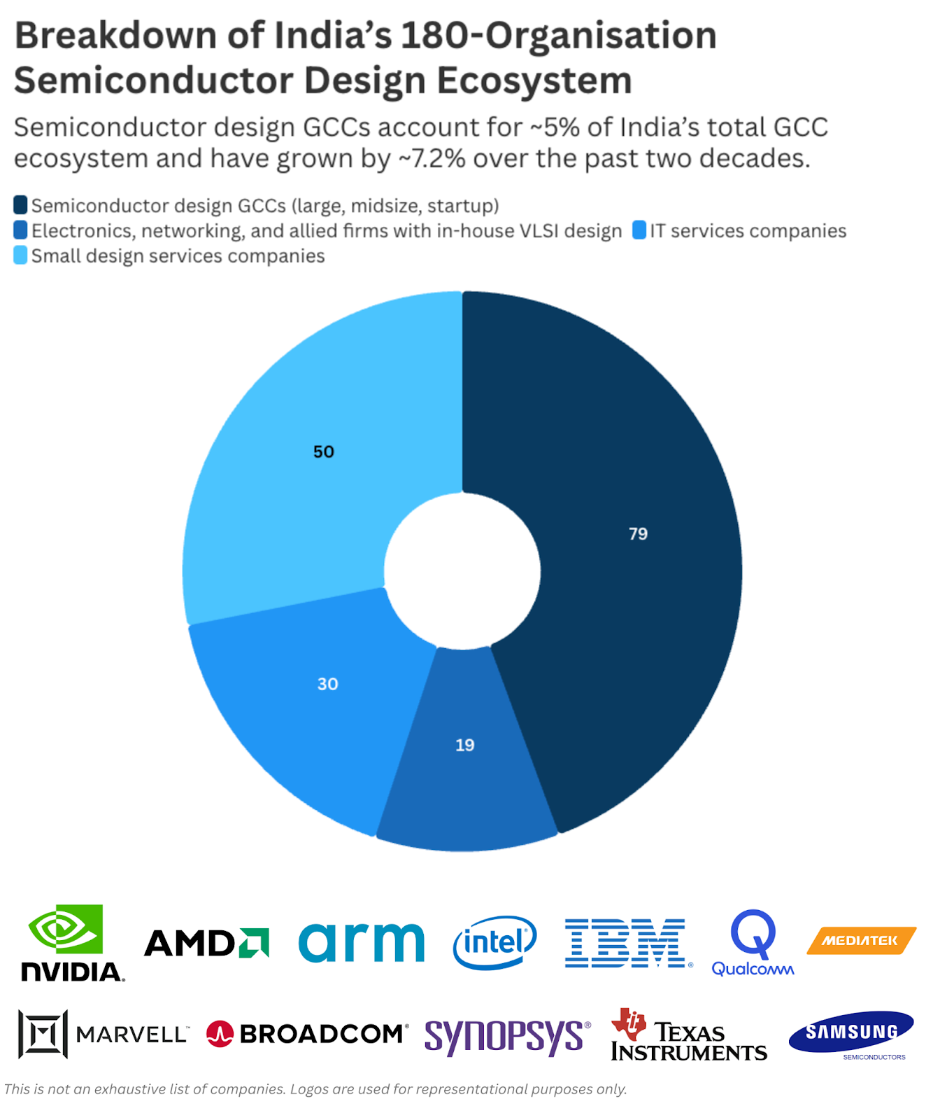
Semiconductor design GCCs account for about 5% of India’s total GCC ecosystem and have grown by approximately 7.2% over the past two decades.
Despite this long-term growth, recent demand trends point to a marked slowdown.
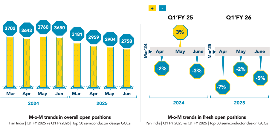
In Q1 FY2025, the top 50 semiconductor design GCCs reported an average monthly demand of 3,684 professionals. By Q1 FY2026, this figure had dropped to around 2,874—a decline of about 22%.
The Careernet report attributes this to a mix of geopolitical tensions, supply-chain disruptions, and heightened uncertainty across global semiconductor markets.
This slowdown is also evident in hiring activity. Active job openings across India’s semiconductor design GCCs declined by 15% in FY2025.
Looking ahead, continued material shortages and restrictions on talent mobility are expected to further reduce advanced role openings through FY2026 and FY2027, slowing project timelines and skill development. Export-linked hiring is particularly vulnerable.
If semiconductor tariffs come into effect, pending the findings of the Section 232 investigation, a significant number of export-oriented jobs could be affected, with direct implications for hiring by multinational firms operating India design centres.
Where Demand Still Exists
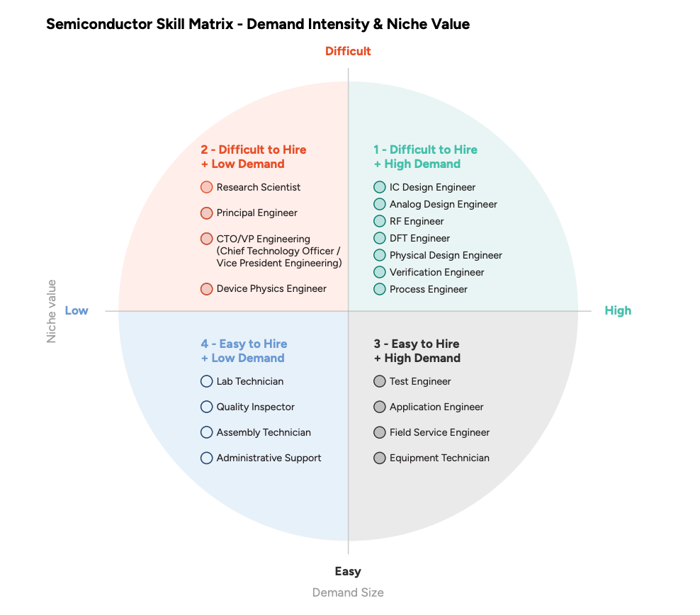
Despite the overall slowdown, hiring demand remains concentrated in specialised roles.
In Q1 FY2026, recruitment across the top 50 GCCs was dominated by core VLSI skills, which accounted for 48%. System and application software roles accounted for 35%, with the remainder spread across business operations and IT support.
Within technical roles, the split was divided between digital design, verification, and system software, all of which continue to see steady demand. The report expects these roles to remain critical as government-backed semiconductor initiatives expand and new design GCCs increase by around 30% by 2030.
Multinational companies dominate high-value roles in India’s design ecosystem. Large global chipmakers control most high-paying design and leadership positions, with senior engineers earning up to about $38,390 annually.
Semiconductor professionals in India earn 25-35% more than those in the broader IT and software sector. At the top end, compensation can reach approximately $90,293 per year, with the highest pay premiums in chip design, AI, ATMP, VLSI packaging, and photolithography.
These salary gaps reinforce the dominance of multinational firms in attracting top talent, while domestic companies struggle to compete on pay alone.
How Global Firms See India
While industry reports capture macro-level hiring trends, industry leaders highlight a different layer of the story—how India fits into global semiconductor workflows and why its talent pool remains strategically important despite near-term hiring volatility.
“India’s semiconductor talent is among the finest in the world, combining technical depth with adaptability,” says Fathima Farouk, head HRBP, India and APJ at AMD, in an interaction with AIM. She states how a global company like AMD hires engineers in India who “work across the full product lifecycle, from architecture to post-silicon validation, contributing to nearly every AMD product globally.”
The story is similar across several global companies that operate design and engineering centres in India.
From a geographic standpoint, about 70% of India’s semiconductor design GCCs serve the Americas. This concentration ties India’s design hiring cycle closely to demand cycles in the US and global technology markets, amplifying the impact of geopolitical shifts and trade policy changes on local employment.
The Talent Gap
India has a large engineering talent base and a growing semiconductor ecosystem. Yet, the gap between academic training and industry requirements remains wide.
India produces roughly six lakh electronics engineering graduates each year, but only a small fraction are considered job-ready for fabrication or advanced chip design roles. Skill development remains the dominant constraint on industry expansion.
At the same time, hiring priorities are shifting as semiconductor manufacturing becomes increasingly data-driven.
Fabrication plants and design centres are increasing recruitment for AI and machine learning engineers, data scientists, chip designers, and cybersecurity specialists. AI-driven manufacturing, predictive analytics, and digital twins are becoming standard across semiconductor operations, reshaping the skill mix required by large firms.
“The future is bright for students entering semiconductor engineering. With AI redefining chip design and verification, opportunities are expanding beyond traditional roles into AI-driven design automation, embedded intelligence, and high-performance computing,” Farouk says.
She also emphasises that engineers in this industry must remain curious about new architectures, designs, automation, and AI-based tools. “Upskilling in system-level integration, low-power design, and AI accelerators will ensure that experienced professionals remain at the forefront of innovation,” she adds.
While recent hiring trends do show a slowdown, Farouk emphasises that semiconductors remain a long-term growth sector. “This is the right time for professionals to invest in learning and broaden their expertise into adjacent areas like AI, machine learning, and software-defined hardware.”