
5 min
 Intel last week revealed their detailed strategy about how to hold all the data-intensive workloads for devices, networks and cloud data centres. They announced the launch of a revolutionary and industry’s first 3D stacking of logic chips. This stacking will be introduced in the market after one year.
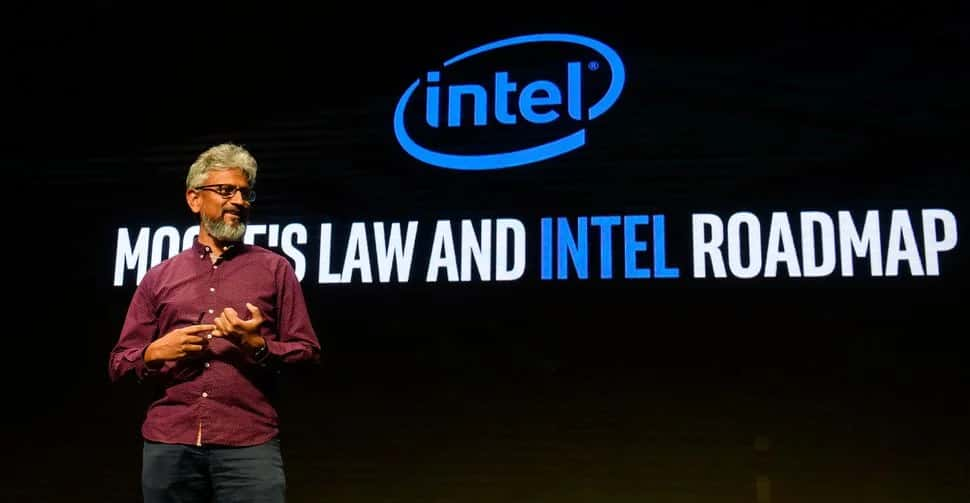
Raja Koduri, Intel chief architect, senior vice president of Core and Visual Computing Group, said, “For an expanding data-centric market, the company has to deliver leadership products across all architectures and workloads.”
The new 3D packaging technology called Foveros is a unique packaging system because while most of the other companies are making micro and nanochips; Intel is stacking up chips and making it 3D. This innovation aims to enable logic-on-logic integration on various systems. According to reports, the chips have gone through rigorous testing, changes in new power delivery process and in the insulation material.
Foveros: For The Core Technology
Foveros packaging will be installed in CPU’s, graphics and AI processors. The stacking is an effective measure to save space (more transistors can be packed in a given space), customize the combination of Silicon to user’s needs and make power delivery better. The technology also provides a platform to “mix and match”; designers can use various memory and “I/O” elements in a device, these processors can be combined into a single package. The vertical approach will boost memory chips in the stack. Intel will launch products with Foveros technology in the second half of 2019. Devices and systems created using these chips will serve the purpose of high performance, high density and low power Silicon technologies to users. According to reports, “Foveros will allow products to be broken up into smaller “chiplets,” where I/O, SRAM and power delivery circuits can be fabricated in a base die and high-performance logic chiplets are stacked on top.” This chiplets help in no power loss and no performance loss.Breaking Barriers: Foveros For The Win
 The 2D stacking has been prominent in the market since it’s inception in 2018, though it has some drawbacks. Patrick Moorhead, CEO of Moor Insights & Strategy said, “The 2D approach allows for some variety, but also sacrifices performance and draws more power. In 3D, there’s virtually no power and performance loss when you put the chips together.” The Embedded Multi-die Interconnect Bridge (EMIB) 2D packaging had a 7 nm base while the chiplet in Foveros will be 10nm with a low-power of 22FL base die.
The primitive technology was the monolith, where functions were integrated on a single base die, this caused high energy loss and performance loss as well. The 2 D technology served the users with better efficiency but the 3D ensures no loss of performance and power. The architecture allows manufacturers to swap in any transistors (according to needs), many devices can perform with orderliness due to stack.
- Coforge Revenue Rises 54% as AI Engineering and Deal Bookings Gain Momentum
- Tech Mahindra Partners With SpaceXSI to Bring AI Into Software Engineering
- Infosys AI Revenue Rises 29% in Q2, FY27 Growth Guidance Cut
- LTM Launches BlueVerse Industrial AI Lab in Chennai
- Chariot Launches Speech Recognition Model for 10 Indian Languages
- Meta Expects Up To $145 Billion In Capex As AI Investments Expand