
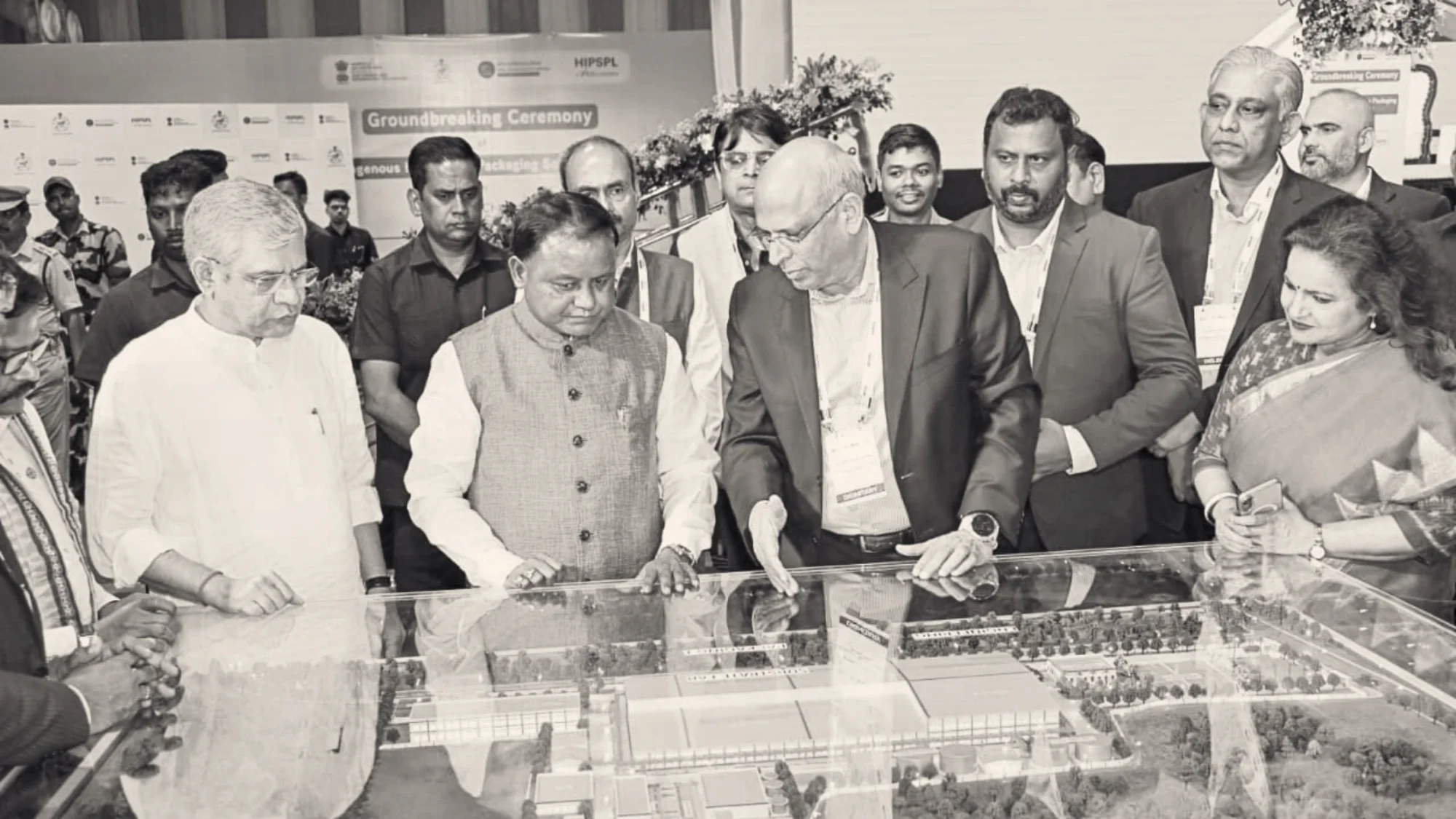
The foundation stone for the first advanced 3D semiconductor packaging unit in India has been laid at Info Valley in Bhubaneswar, Odisha. The project, promoted by 3D Glass Solutions through its Indian subsidiary, aims to strengthen the country’s semiconductor ecosystem and support high-end electronics manufacturing.
This facility was announced by the Union Cabinet in early December last year, alongside three other facilities in Odisha, Andhra Pradesh, and Punjab, under a total outlay of ₹4,600 crore.
The facility will focus on heterogeneous integration packaging, and the project was announced with an investment of ₹1,943 crore, including central and state support. The facility is expected to produce 70,000 glass panels each year, along with 50 million assembled units and around 13,000 advanced modules.
Union Minister Ashwini Vaishnaw said that two semiconductor projects have already been approved for Odisha under the India Semiconductor Mission, with three more proposals in progress. Discussions are also underway with global firms, including Intel, for future investments.
Commercial production is scheduled to begin in August 2028, with full-scale output targeted for August 2030. The unit will cater to data centres, machine learning, AI, defence, 5G and 6G communications, automotive systems, aerospace, and photonics.
Odisha Chief Minister Mohan Charan Majhi said in a statement that the project marks “a historic milestone for Odisha and the nation”. He added that the state is ready to support the goal of making India self-reliant in semiconductor manufacturing.
He said the project would create employment opportunities for engineering graduates, diploma holders, and ITI students. He also noted that Odisha is the only state hosting both a compound semiconductor fabrication unit and a 3D glass substrate packaging facility.
https://www.youtube.com/watch?v=vTFTu_daoHg
Vaishnaw said India’s semiconductor sector is seeing growth, and Odisha is becoming an important contributor. “India has now become the world’s second-largest mobile phone manufacturer and emerged as the leading exporter of mobile phones in 2025,” he said.
The minister said the project would strengthen India’s semiconductor value chain and support growth in electronics manufacturing. He also pointed to ongoing infrastructure investments, including railway projects, to support industrial expansion in the state.
State officials said Odisha’s policies in IT, AI, and semiconductors aim to attract investment and build a skilled workforce. The project forms part of a broader push to develop the state as a centre for electronics and semiconductor manufacturing, alongside the state’s efforts to pursue a stronghold on the drone ecosystem.

Your reaction
Discussion
What's your take on this story?
No comments yet — be the first to share your view.