

India’s first semiconductor push was largely about getting fabs, packaging units and chip-design capabilities off the ground. The next phase is about filling the gaps around them, from semiconductor equipment and materials to advanced packaging, research and talent.
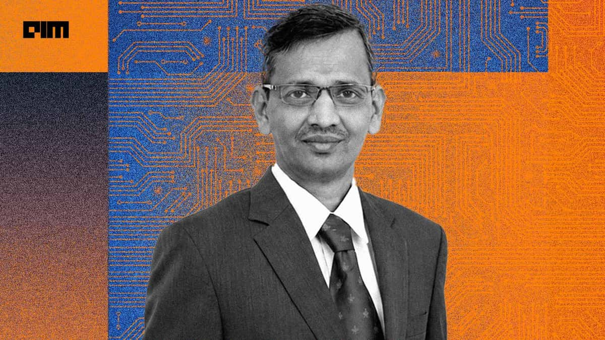
That is the view of SD Sudarsan, Executive Director at C-DAC Bengaluru, who believes the next stage of India’s semiconductor journey will be about building the capabilities required to make the entire semiconductor stack work inside the country.
In an exclusive interview with AIM about the transition from India Semiconductor Mission (ISM) 1.0 to ISM 2.0, Sudarsan says the second phase is about scaling existing efforts while moving deeper into the semiconductor value chain.
The Union Cabinet approved the expanded Semicon 2.0 programme in July with a total outlay of ₹1.275 lakh crore. It is built around six pillars covering chip design, equipment and materials, fabs, advanced packaging, R&D and talent development.
Sudarsan says ISM 2.0 builds on the initiatives under the first phase, particularly those involving academia and startups, while increasing their scale and reach.
But the bigger shift, according to him, is the move towards a manufacturing ecosystem, including semiconductor fabs, OSAT and ATMP facilities, as well as the materials needed to operate them.
From Supporting Fabs to Building the Ecosystem Around Them
India’s first semiconductor push has already resulted in multiple projects.
For instance, in Dholera, Gujarat, Tata Electronics is developing a semiconductor fab in partnership with Taiwan’s Powerchip Semiconductor Manufacturing Corporation (PSMC), with an investment of around ₹91,000 crore. The fab will have a capacity of 50,000 wafer starts per month and will manufacture chips for applications including automotive, mobile devices, AI and other sectors.
In Assam, Tata Electronics is building a ₹27,000-crore semiconductor assembly and test facility in Jagiroad, Morigaon.
Sudarsan says that having fabs is only one part of becoming a semiconductor manufacturing country.
“Materials are very critical because a fab typically requires hundreds of unique chemicals,” he says, mentioning that many of these materials fall under different regulatory categories, including hazardous substances, import restrictions and export controls.
For India, this creates a new challenge. The country has to develop the expertise and infrastructure required to handle semiconductor materials at scale, rather than depending entirely on imports.
He compares this progression with the National Supercomputing Mission. India initially worked on system design, then moved to server design and manufacturing, and is now working towards designing processors and other components domestically.
He says that this brings the semiconductor mission and the National Supercomputing Mission into closer alignment, with capabilities developed under each initiative supporting the other.
India Has Chip Design Talent
Speaking to Morgan Stanley, Union Electronics and IT Minister Ashwini Vaishnaw said India now accounts for 20% of the global semiconductor design workforce.
“Some of the most complex tasks take place at the design level itself. We set a target of developing a pool of 85,000 skilled engineers in 10 years,” Vaishnaw wrote in his Substack post recently.
According to Sudarsan, around 25–30% of global chip design activity is carried out in India, although much of that work happens through global companies’ engineering centres and GCCs.
The challenge is turning that design capability into Indian-owned products.
“India is very good with front-end design. We have enough talent,” he says. “But after the blueprint or the architecture is done, now you have to achieve it in real implementation.”
That implementation requires what is commonly referred to as back-end design, where engineers have to translate a chip architecture into something that can actually be manufactured in a particular fabrication process.
Sudarsan believes India is beginning to close that gap.
One indication is the growing sophistication among students and engineers working on chip design. He recalls that five years ago, discussions around VLSI design in academic institutions were relatively broad. Today, engineers increasingly distinguish between front-end and back-end design and specialise in areas such as analogue, digital, RF and mixed-signal design.
“That means the technical depth is increasing, and this is what is giving us the confidence,” he says.
The talent challenge is not simply about hiring more engineers.
Sudarsan argues that manufacturing requires a different mindset, one built around ownership, discipline and consistency.
For India, that cultural shift could matter just as much as government funding or infrastructure.
ISM 2.0 could Bring Investors into the Equation
One particularly interesting feature of ISM 2.0 is equity co-investment.
ISM CEO Amitesh Kumar Sinha said the government plans to co-invest alongside eligible private/VC investors and take an equity position in semiconductor startups. The intention is to eventually exit those investments as companies mature, allowing the public capital to potentially be recycled into other semiconductor startups.
Sudarsan says ISM 2.0 is exploring ways to support more complex and capital-intensive designs where conventional support may not be enough.
One proposal under consideration is a matching grant mechanism. If a venture capital fund or angel investor conducts due diligence and invests in a semiconductor company, the government could potentially match that investment.
“The thought process is if I can generate VC funding of X amount with government matching, it will become 2X,” Sudarsan explains.
The significance goes beyond simply putting more money into startups. It would bring commercial due diligence into the funding process.
“It has become a techno-economic feasibility in the new scheme,” Sudarsan says.
India’s Fabs
The semiconductor projects already approved by the government are still several years away from becoming fully operational, and Sudarsan says he is not aware of any delays affecting those timelines.
ISM 1.0 has approved 12 semiconductor projects with investments of more than ₹1.64 lakh crore, including Micron’s packaging facility, Tata Electronics’ silicon fab with PSMC, and OSAT projects by CG Power and Kaynes Semicon.
He adds actual production is expected only in 2028–29.
For India, that makes the next few years particularly important. The country is not simply waiting for its first fabs to become operational. It is also using the experience of setting them up to reduce the time and complexity involved in future projects.
“With ISM 2.0, more and more fabs coming in, the time to set up those fabs may be slightly less because now we have the experience of setting up one process,” he says.
What India can learn from Taiwan
The comparison with Taiwan inevitably comes up when discussing semiconductors. TSMC has become the world’s most prominent contract chip manufacturer, while India is still building the foundations of its domestic manufacturing capability.
But Sudarsan does not frame India’s journey as a case of having made a mistake compared with Taiwan.
He points to the importance of sustained technological capability and the ability to build domestic expertise when external circumstances demand it.
The growth in applications under the Design Linked Incentive ecosystem is another sign of this change.
Sudarsan says the initial target was to support 100 chip-design applications, but it took nearly two years for the first two companies to come under the scheme.
The number has since crossed 100.
“In less than three years, we have moved from two to 102,” he shares.
He attributes this acceleration to the Design Linked Incentive Scheme, which has reduced technology and licensing barriers by giving startups access to advanced EDA tools, while technical evaluation helps them assess whether their proposed chip designs are feasible.
Sudarsan recalls how India’s supercomputing programme emerged after the country faced technology restrictions in the 1980s. That period led to the creation of C-DAC and the development of the Param supercomputer.
But maintaining that momentum is harder when technology becomes readily available from elsewhere.
That is where semiconductors could be different this time. With AI, geopolitical tensions and supply-chain concerns making advanced computing hardware strategically important, India has a stronger incentive to develop domestic capabilities.
For India to eventually manufacture cutting-edge chips, simply establishing fabs will not be enough.
Vaishnaw said India now has 40 nm chip manufacturing capabilities and will develop a clear roadmap to reach advanced nodes ranging from 7 nm to 3 nm over the next eight years.
Sudarsan identifies several layers that need to mature before India can seriously target leading-edge manufacturing.
Materials are one. Semiconductor equipment is another.
“When you talk of 2 nanometers or something like that, the equipment should be of that kind of high quality, high precision,” he says.
Pointing to TSMC as an example, he says India needs to develop the same relentless focus on consistency and precision in manufacturing.
For Sudarsan, manufacturing excellence is fundamentally different from research capability. India has demonstrated strength in research, engineering and software. Semiconductor manufacturing, however, requires processes that deliver the same result repeatedly and with extremely high precision.
That may ultimately be one of the biggest tests for India’s semiconductor ambitions. Designing an advanced chip is one challenge. Producing millions of them with consistently high yields is another.
The natural comparison for India is often a single national champion, whether it is Huawei in China or TSMC in Taiwan.
Sudarsan does not believe India necessarily needs to reproduce that model.
He argues for a much broader base of semiconductor companies, including smaller and specialised manufacturers. “Instead of one top company, we need hundreds and 1000s of companies across the continent, across the domains,” he says. “I personally believe in the future India should look at micro factories.”
These smaller factories could specialise in specific products or applications rather than trying to build one massive company that dominates the entire market.
Indigenous GPUs
The semiconductor push also intersects directly with India’s ambitions in sovereign AI.
India has been building foundation models and AI software, but foreign processors and accelerators dominate the hardware underneath those systems.
C-DAC is now working to change that.
The organisation has developed indigenous RISC-V-based processors, including 32-bit and 64-bit designs, and has taped out multiple chips. Startups and academic institutions use its development boards for applications ranging from drones and image processing to radar and automobiles.
C-DAC is also working on a broader family of processors, GPUs and AI accelerators. It is developing an indigenous GPU that could be launched by 2029, aiming to match the performance of competing products available by then.
He adds that the target is to develop an indigenous chip comparable to other GPUs available in the market at the time. “By then, the workloads would have changed because new algorithms, new innovations, new models will be there,” he notes.
The Bigger semiconductor bet
India’s semiconductor strategy is therefore becoming less about whether the country can build a fab and more about whether it can build an ecosystem around that fab.
ISM 1.0 helped establish the initial momentum around design, startups and manufacturing projects. ISM 2.0, as Sudarsan describes it, is intended to push that ecosystem deeper into materials, equipment, fabs, packaging, specialised design and larger commercial opportunities.
India’s current semiconductor projects include a significant focus on OSAT and ATMP, which cover packaging and testing after a chip has been fabricated.
Sudarsan stresses that these are important parts of the semiconductor value chain, but they should not be mistaken for the endpoint of India’s ambitions.
Moving towards advanced fabs will require simultaneous progress in materials, equipment, process control and manpower.
The real test will come when India has to manufacture at scale, maintain yields, develop advanced equipment, train highly specialised workers and turn domestically developed IP into products that can compete beyond the Indian market.
And if India can build that network at scale, Sudarsan believes its semiconductor future does not have to depend on finding a single company that becomes the country’s TSMC.
- Smaller Language Models Could Reshape How Enterprises Deploy AI
- Enmovil Plans to Quadruple FDE Team as Enterprise AI Hiring Moves Beyond Coding
- Does the World Need a New GitHub?
- Can India’s AI Boom Reach Bharat?
- AI's Next Agritech Frontier Is India's Fragmented Supply Chain
- India’s Frontier AI Race Gets a 240M Model That Beats Liquid AI