
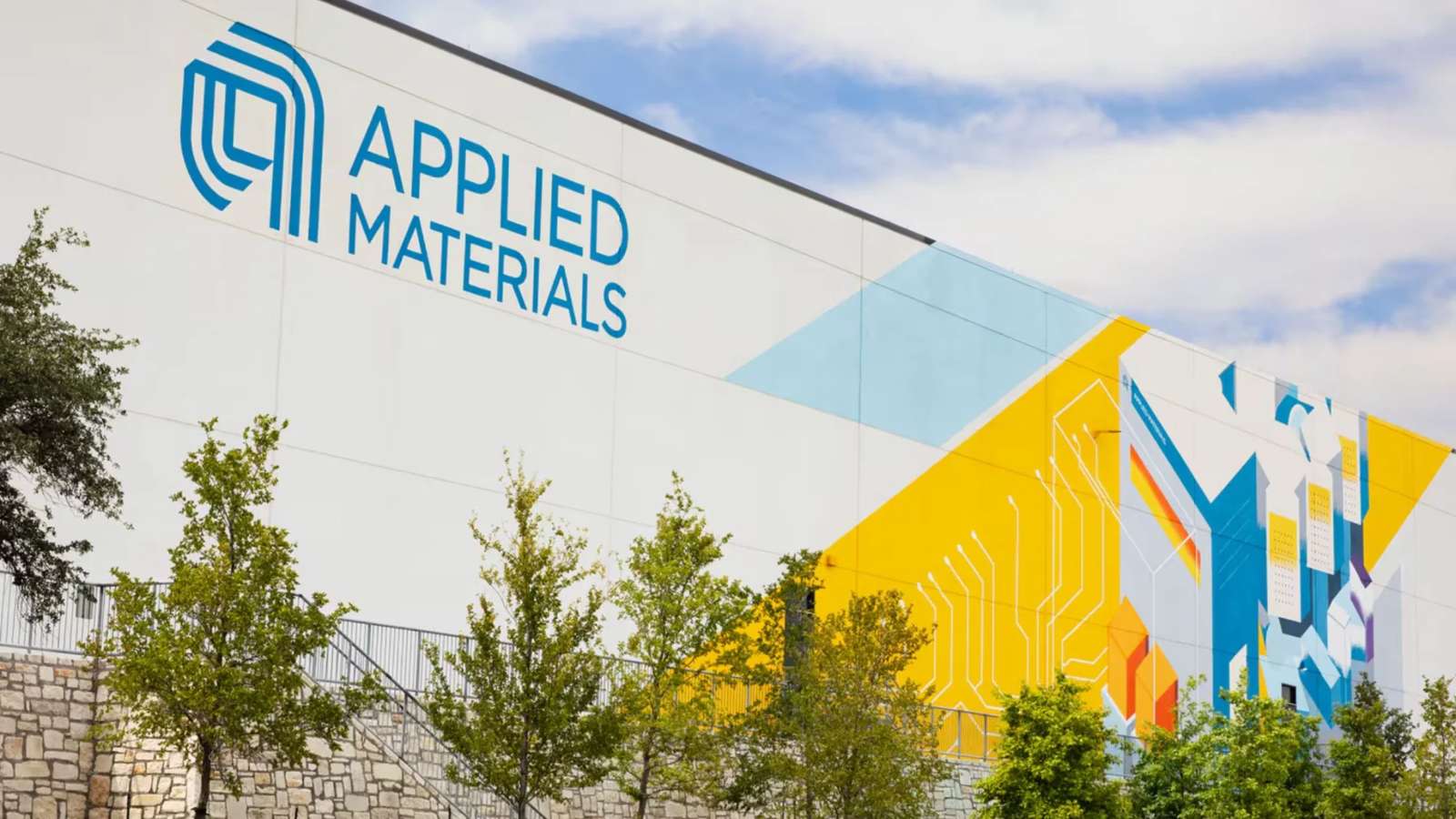
Applied Materials and Intel Corporation have partnered to accelerate next-generation semiconductor development for AI computing. The collaboration will focus on transistors, interconnects, and advanced packaging.
The companies will work across Applied Materials’ EPIC (Equipment and Process Innovation and Commercialisation) Center in Silicon Valley and Intel’s research and development (R&D) campus in Hillsboro, Oregon, to shorten development timelines.
The partnership aims to address growing demand for AI computing by improving chip performance, power efficiency, and packaging. Both companies will develop materials, manufacturing processes, and device architectures for advanced logic nodes that target AI workloads.
They will also work on packaging technologies for Intel’s Foveros-based 3D chip stacking.
This builds on decades of collaboration between the two companies on semiconductor scaling challenges and covers both front-end and back-end manufacturing processes, including interconnect scaling.
The work also aims to increase interconnect density, improve power delivery, and enhance thermal performance for high-performance computing systems.
“Bringing our teams together at the EPIC Center will deepen that partnership and accelerate the transistor, interconnect and packaging innovations needed to drive the future of AI computing,” Gary Dickerson, President and CEO of Applied Materials, said in a statement.
Intel CEO Lip-Bu Tan added that demand for AI computing requires advances in performance, power efficiency, and packaging. He said that the company wanted to expand its work with Applied Materials to accelerate the transition from research to high-volume manufacturing in the United States.
Applied Materials’ EPIC Center is scheduled to become operational this year. The facility aims to shorten the time it takes to move semiconductor technologies from early-stage research to full-scale manufacturing.
The centre will give chipmakers earlier access to Applied Materials’ research portfolio and support faster testing and development cycles. It will also help transfer new technologies into high-volume manufacturing through a secure collaborative environment.
Prabu Raja, President of Applied Materials’ Semiconductor Products Group, said closer collaboration between research and manufacturing teams had become essential as semiconductor development grew more complex.
The companies expect their joint work at the EPIC Center to shorten development cycles and bring new technologies to market faster. Applied Materials also expects the centre’s co-innovation programmes to improve research productivity and guide investment across multiple semiconductor process nodes.
Naga Chandrasekaran, Executive VP, Chief Technology and Operations Officer, and general manager of Intel Foundry, said accelerating R&D was critical to meeting the demands of expanding AI infrastructure.
He said the EPIC Center would let companies work more closely on materials development and process innovations, supporting Intel Foundry’s manufacturing and technology goals.
- Anthropic Posts $17 Bn in Q3 Revenue, Swings to Operating Loss
- OpenAI Signs Four Agreements With Abu Dhabi Across Government, Energy And Investment
- Deep-Tech and Green Finance to Drive India’s Climate Investments in 2027
- Google’s Project Suncatcher Satellite Generates First AI Response in Orbit
- DeepSeek Proposes Super-Agent Architecture to Automate AI Coding Workflows
- Arrowhead AI Launches Fletch Voice Model for Multilingual Customer Calls