


With the rise of hybrid clouds, artificial intelligence, and the Internet of Things, chip performance and energy efficiency are becoming more important. However, each decade tests the limits of Moore’s Law, and the twenty-first century is no exception. This new 2 nm chip, which was designed and manufactured at IBM’s Albany research facility, has a 100,000 square foot room that helps advance the semiconductor industry, meeting the needs of the growing market. Using IBM‘s nanosheet technology, it is projected to achieve 45 per cent higher performance or 75 per cent lower energy consumption than today’s most advanced 7 nm node chips. In addition, this 2 nm chip demonstrates the capability to scale semiconductors. IBM announced its landmark 5 nm design less than four years ago, and this latest breakthrough allows for a chip the size of a fingernail to incorporate 50 billion transistors.
A new era of fabrication: 2nm
Although the process node is termed ‘2 nanometers’, nothing about transistor dimensions resembles what might be expected from 2nm. For the past few years, the dimension has been used as an equivalent metric to measure the size of the 2D features on the chip. Today, with the advent of 3D transistors such as FinFETs and others, the process node name interprets a 2D equivalent transistor. Now, through these FinFET/nanosheet technologies, the voltage characteristics of individual transistors can be customised.
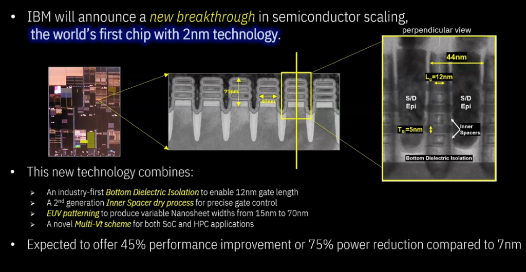
It is certainly true that some of the features on this chip are likely to be low single digits in actual nanometers, such as transistor fin leakage protection layers. IBM images reveal that this new 2nm processor uses a three-stack GAA design. Regarding the development of Gate-All-Around/nanosheet transistors, IBM’s 3-stack GAA uses a cell height of 75 nm and cell width of 40 nm, 5nm wide, and 5nm high nanosheets. The gate length is 12 nm, and the gate poly pitch is 44 nm. IBM claims its design is the first to use bottom dielectric isolation channels, enabling a gate width of 12 nanometers. Its inner spacers are a second-generation dry process design, which helps enable the development of nanosheets. In addition, for the first time, EUV patterning has been applied to the FEOL parts of the process, enabling EUV to be used at all stages of the design.
As semiconductor device fabrication processes have evolved, extreme ultraviolet (EUV) lithography uses UV light to produce a pattern by exposing a reflective photomask to UV light, which is reflected onto a substrate covered with photoresist and is now used to fabricate devices. Even though IBM has not released details about the 2nm test chip, it’s likely to be a simplified SRAM test platform with a little logic. The 12-inch wafer images show various light diffraction patterns, which might indicate a variety of tests to confirm the technology’s viability. For high-performance and high-efficiency application demonstrations, IBM says it uses a multi-VT scheme. With this and other advancements in technology, transistor sizes can decrease, enabling the future of semiconductors. Despite this, chipmakers have continued to advance transistor technologies, but interconnects in these structures have been lagging.
IBM at the forefront of semiconductor innovation
Along with this 2nm chip, IBM also pioneered 7nm and 5nm process technologies, single-cell DRAM, chemically amplified photoresists, copper interconnect wiring, Silicon on Insulator technology, multi-core microprocessors, High-k gate dielectrics, embedded DRAM, and 3D chip stacking. This year, IBM released a POWER10-based IBM Power System that incorporates IBM Research 7nm advances. As the semiconductor industry continues to innovate, we will be particularly interested in how this can lead to cloud providers or other large-scale data centre operators using fewer servers to accomplish the same amount of work while reducing energy costs and carbon footprints.