
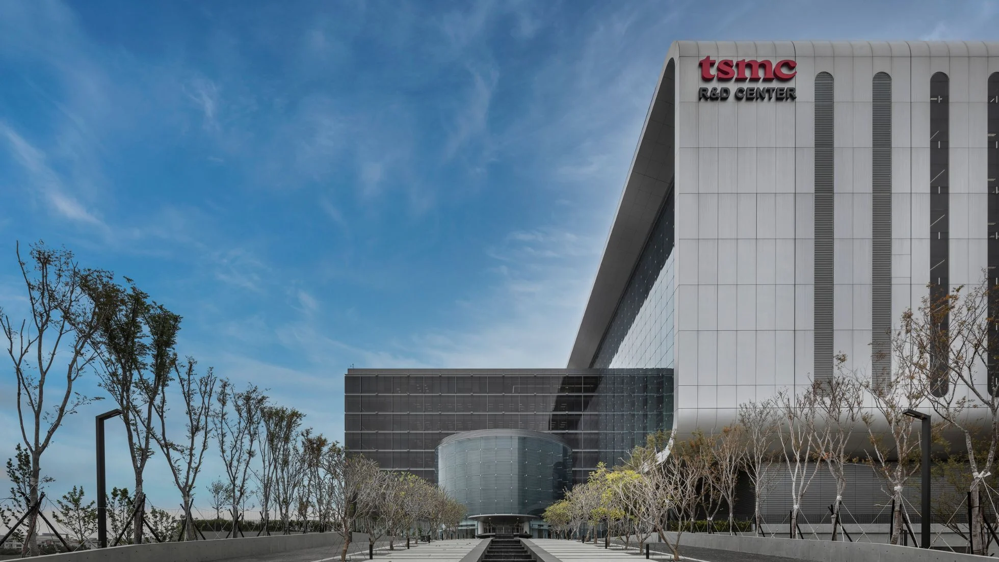
For years, the semiconductor industry has followed a rhythm in which a new node would arrive, and chips would get smaller and faster. But many are wondering if TSMC is changing—or maybe even stretching—that rhythm as the industry faces a high demand for chips to sustain AI workloads.
At its North America Technology Symposium in Santa Clara, TSMC introduced its A13 process technology as it looks to meet rising demand for AI, high-performance computing, and mobile applications. But the new node builds on its A14 process and will only enter production in 2029, one year after A14.
With this, the world’s largest semiconductor foundry is signalling that companies must now plan far ahead before it fulfils their computing needs. At the same time, AI workloads are evolving faster than chip cycles, packaging is becoming as critical as transistor scaling, and design itself is turning into a software problem.
“At TSMC, we understand our customers are always looking ahead to their next innovation,” said CEO CC Wei in a statement announcing the A13 node. “They come to us for a reliable stream of new silicon technologies.”
In that context, A13’s unveiling comes at a time when the industry is learning to design for a world it cannot yet fully predict, where the real challenge is not building better chips but making sure the timing of production aligns with the needs.
The company said A13 offers a 6% area reduction compared with A14 and maintains backward compatibility with A14 design rules, enabling customers to migrate designs more quickly. It also improves power efficiency and performance through co-optimisation of design and technology.
TSMC positioned A13 as part of its roadmap to address growing compute needs driven by AI workloads. The company said customers are seeking compact and efficient chip designs to support next-generation applications.
New Fronts
At the symposium, TSMC also introduced updates across its technology stack. It previewed A12, an enhancement to the A14 platform that includes backside power delivery through Super Power Rail technology, which reduces power loss by 20%. The company said A12 is also scheduled for production in 2029.
TSMC advanced its 2nm platform with N2U, which delivers 3–4% speed gains or 8–10% power reductions, along with marginal density improvements. The company plans to bring N2U into production in 2028. This was also addressed in the company’s latest quarterly earnings report, where it discussed trust in 2nm technology despite it slashing revenue margins.
In advanced packaging, TSMC said it is expanding its Chip-on-Wafer-on-Substrate (CoWoS) technology to support larger chip integrations. The company is developing a 14-reticle CoWoS platform capable of integrating about 10 compute dies and 20 high-bandwidth memory stacks, with production expected in 2028. Further expansion beyond this scale is planned for 2029.
The company is also advancing its System-on-Wafer (SoW-X) technology, which is expected to support large-scale integration for AI workloads by 2029. It is also advancing its 3D chip-stacking technology, with an A14-based SoIC expected to deliver higher interconnect density for data transfer.
In photonics, TSMC said its COUPE platform will enable co-packaged optics by integrating optical engines directly within chip packages. This is set to begin production in 2026. The company said this approach delivers up to 2x power efficiency and reduces latency by up to 10x compared to pluggable optical solutions.
Beyond AI, TSMC highlighted developments in automotive and speciality technologies.
Its N2A process, which it described as its first automotive-grade nanosheet technology, will target automotive applications and is expected to complete qualification in 2028. Meanwhile, in speciality technologies, TSMC highlighted its N16HV process for display driver applications.
The company said it improves gate density and reduces power consumption compared to earlier nodes, while enabling smaller, more efficient designs for smartphone displays and near-eye devices such as smart glasses.
Expands Design with Cadence
Alongside the technology announcements, the chip foundry giant also expanded its collaboration with Cadence Design Systems, specialising in electronic design automation, to support AI chip design across advanced nodes, including N3, N2, A16, and A14.
The partnership focuses on delivering design infrastructure, IP, and certified flows to reduce iterations and improve time to tapeout. Cadence said it is developing “agent-ready” design flows that integrate AI to optimise power, performance, and reliability.
“Through collaboration with TSMC, we’re advancing our Design for AI and AI for Design strategy,” said Chin-Chi Teng, Senior VP and GM of the Digital and Signoff Group of Cadence.
The companies said customer activity on 3nm and 2nm nodes continues to grow, reflecting demand for advanced semiconductor technologies and integrated design ecosystems.
Cadence said its collaboration with TSMC also extends across a wide range of certified design tools aligned to advanced nodes such as N2 and A16. It centres on 3D-IC and heterogeneous integration.
Industry players said the collaboration will support evolving AI chip requirements.
“By collaborating with Cadence, NVIDIA is helping advance the EDA tools necessary for its design teams and the global semiconductor ecosystem,” said Tim Costa, Senior Director of CAE, Quantum and CUDA-X at NVIDIA.
Positron CTO Thomas Sohmers also mentioned using Cadence IP and tools on TSMC’s advanced nodes to build its AI inference accelerator.

Your reaction
Discussion
What's your take on this story?
No comments yet — be the first to share your view.