
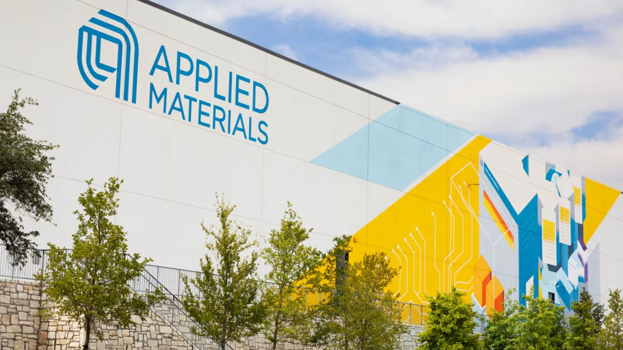
Applied Materials has signed a definitive agreement with ASMPT Limited to acquire its NEXX business, a supplier of advanced packaging deposition equipment for the semiconductor industry.
The company announced the deal in India and said it expects to close it in the next several months, subject to customary conditions. No regulatory approvals are required.
The acquisition will add NEXX’s panel-level electrochemical deposition technology to Applied Materials’ portfolio. The company said the move will support growing demand for larger and more complex AI chip packages.
With this deal, the NEXX team will join Applied’s Semiconductor Products Group and remain based in Billerica, Massachusetts.
Applied Materials said rising AI workloads are increasing demand for chiplet-based designs. These designs integrate GPUs, high-bandwidth memory, and input-output chips into a single package. The company added that advanced architectures such as 2.5D and 3D stacking require larger interposers and substrates.
It said this shift is driving a transition from 300-millimetre wafers to larger panel formats. These formats can reach sizes of 510 by 515 millimetres or more. The change enables higher output and larger chip designs.
Applied Materials said it already offers systems across digital lithography, physical vapour deposition, chemical vapour deposition, and etch. It also provides eBeam metrology and inspection tools. The addition of NEXX’s technology will expand its offerings and address a larger market.
“Having NEXX join Applied Materials complements our leadership in advanced packaging, particularly in panel processing,” said Prabu Raja, President of the Semiconductor Products Group at Applied Materials, in a statement.
ASMPT NEXX President Jarek Pisera added that the deal will support the adoption of large-format packaging technologies. Applied Materials also added that the acquisition will help it develop co-optimised solutions for fine-pitch wiring.
It said that this will support advanced packaging roadmaps for chipmakers and systems companies. The company said forward-looking statements in the announcement are subject to risks and uncertainties. These include the ability to complete the transaction and integrate operations.

Your reaction
Discussion
What's your take on this story?
No comments yet — be the first to share your view.