
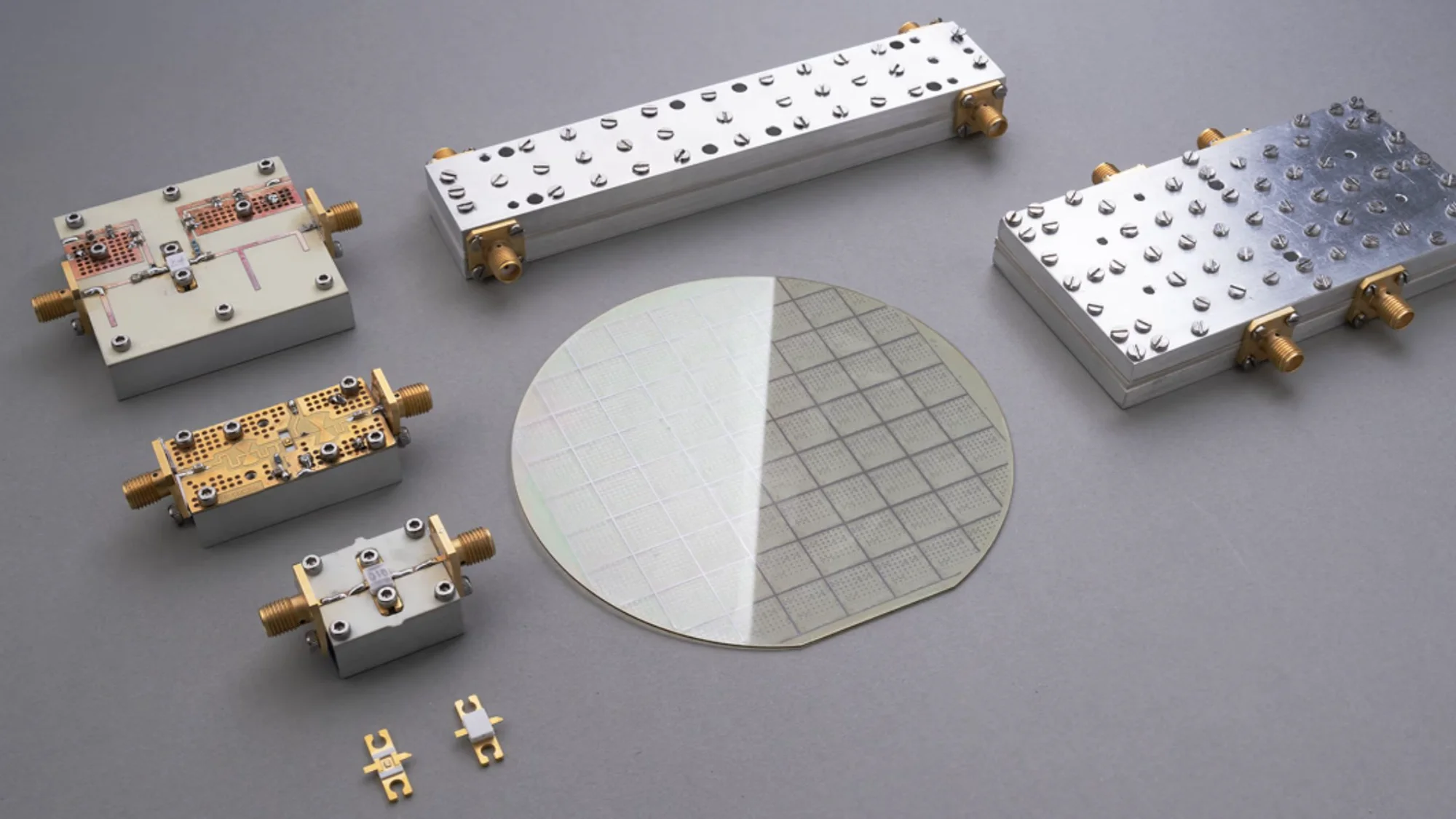
Bengaluru-based semiconductor startup AGNIT Semiconductors has raised $2.6 million in a seed extension equity round led by Shastra VC. Existing investors 3one4 Capital and Zephyr Peacock India also participated in the round.
The funding will support the company’s plan to scale Gallium Nitride (GaN) component production to one lakh units over the next 24 months and expand into telecom infrastructure and power semiconductor devices.
The startup plans to advance its pilot products to volume manufacturing, with commercial shipments of its first strategic products expected to begin in July 2027.
AGNIT said the new capital will help it transition from technology validation to scaled manufacturing. CEO and Co-Founder Hareesh Chandrasekar said the round comes as the company prepares to move its research into commercial systems.
“What excites me most is seeing the science move into real systems, with three distinct radio-frequency products already in pilots across Indian strategic defence platforms,” Chandrasekar said.
He added that the company’s GaN technology is based on over 15 years of research at the Indian Institute of Science. AGNIT has raised $7.47 million in total funding so far. The company plans to expand its presence in radio-frequency chips and high-performance power devices.
The company is targeting opportunities in India’s radio-frequency and power electronics sectors. These segments together represent an estimated addressable market of about $950 million for GaN components.
Ashis Nayak, Founding Partner at Shastra VC, said GaN is becoming an important technology for modern electronics. “From advanced radar systems to next-generation telecom infrastructure, GaN-based chips enable better power efficiency and smaller form factors,” he said.

Nayak added that AGNIT’s vertically integrated approach allows control over wafer manufacturing, device design, and chip fabrication. This structure enables faster research cycles and product development.
In the global race for GaN, TSMC also announced its exit from GaN foundries, leaving PSMC as the world’s largest GaN fab.
The company was incubated at a GaN ecosystem centre at the Indian Institute of Science, supported by the Ministry of Electronics and Information Technology. It has also signed an agreement under the Ministry of Defence’s iDEX programme to develop GaN-based wireless transmitters.

Your reaction
Discussion
What's your take on this story?
No comments yet — be the first to share your view.