
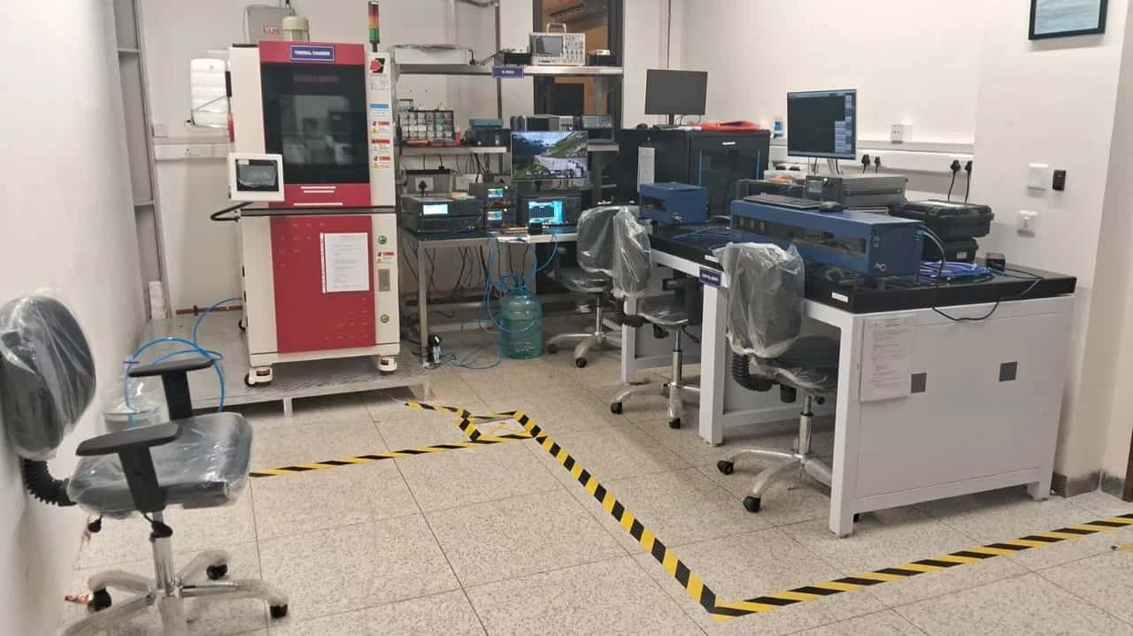
Bengaluru-based semiconductor startup AGNIT Semiconductors has invested ₹3 crore ($300,000) to launch a gallium nitride (GaN) testing and qualification laboratory at the Indian Institute of Science (IISc) in Bengaluru.
The company unveiled the 350 sq ft facility to support in-house validation and reliability testing for high-power radio-frequency (RF) applications in telecom and defence. This comes just after the company raised $2.6 million in a seed extension equity round in March this year.
“India’s semiconductor ambitions require not only chip design and fabrication capabilities but also robust indigenous validation and reliability ecosystems,” said Hareesh Chandrasekar, Co-founder and CEO of AGNIT Semiconductors, in a statement.
The company aims to manufacture 100,000 chips over the next 24 months.
It said the facility will help reduce dependence on external testing infrastructure and speed up the commercialisation of indigenous GaN technologies. The laboratory will support applications across telecom, satellite communications, next-generation wireless systems, and defence.
The lab also houses equipment for testing and pre-qualification of GaN semiconductor components. These include an environmental chamber that operates between -60°C and 125°C, RF test and measurement benches, a connectorised load-pull testing station, and automated PCB assembly systems.
AGNIT said the infrastructure will allow it to conduct PCB assembly, power amplifier board characterisation, reliability data generation, and in-house qualification testing.
The company expects the facility to help move products more quickly from development to deployment and to support changing telecom and defence requirements.
Until now, AGNIT has relied on shared infrastructure at IISc for testing and validation. The new laboratory will allow closer integration with its design and fabrication teams. A dedicated team of five to eight engineers and researchers will run the facility.
AGNIT also plans to expand the laboratory to conduct accelerated lifetime testing and qualification for military-grade components. The company said the move could strengthen reliability testing for semiconductor products developed in India.
Founded as a GaN semiconductor company focused on radio-frequency applications, AGNIT has raised a total of ₹60 crore ($6.2 million) from investors, including 3one4 Capital and Zephyr Peacock, with participation from Lakshmi Narayanan, former Cognizant CEO and angel investor.
- Musk Says SpaceX Closed $40 Bn GPU Debt Deal, Warns Most Neoclouds Won’t Survive
- Coforge Revenue Rises 54% as AI Engineering and Deal Bookings Gain Momentum
- Tech Mahindra Partners With SpaceXSI to Bring AI Into Software Engineering
- Infosys AI Revenue Rises 29% in Q2, FY27 Growth Guidance Cut
- LTM Launches BlueVerse Industrial AI Lab in Chennai
- Chariot Launches Speech Recognition Model for 10 Indian Languages