
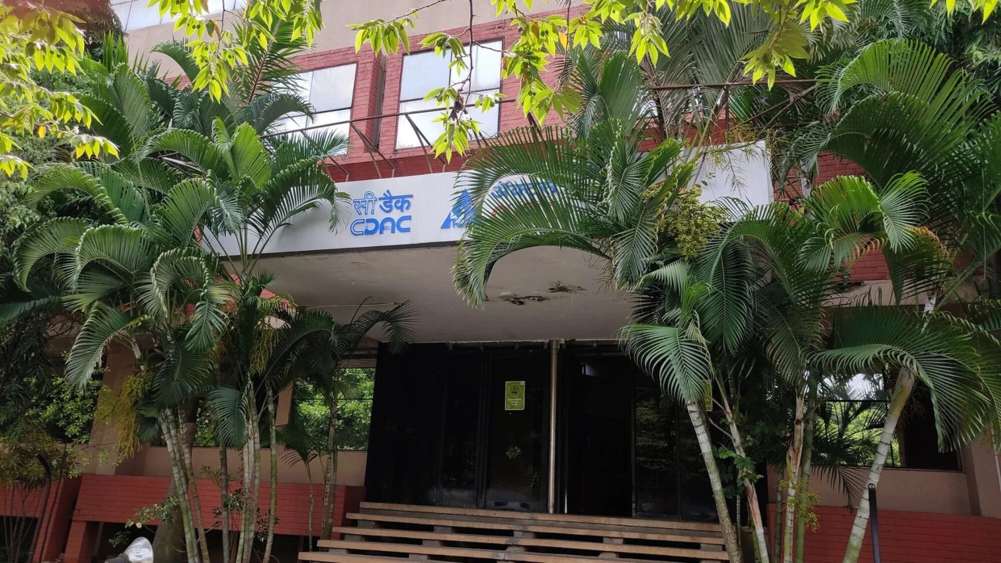
India opened its largest pre-silicon chip validation facility at the Centre for Development of Advanced Computing (CDAC) in Bengaluru to support chip design. Secretary of the Ministry of Electronics and Information Technology, S Krishnan, inaugurated the PRITVI-ACE platform to support national R&D and startups.
The system uses Siemens EDA’s Veloce Pro FPGA platform and AMD Xilinx VP1942 FPGAs. The facility aims to improve first-silicon success rates and cut development costs through early testing and validation.
CDAC said the facility enables near-silicon-speed prototyping and system-level validation before fabrication. Officials said the platform supports early operating system boot, firmware checks and performance benchmarking.
According to reports, Krishnan said PRITVI-ACE will function as a national shared resource for strategic programmes and academic institutions. It will support the National Supercomputing Mission, the India Semiconductor Mission, as well as the Chips to Startups initiative and the DLI scheme.
The platform can validate designs for 48-core high-performance processors (HPCs) and can also support multiple smaller designs in parallel. CDAC officials said this will support indigenous development in HPCs, AI, and networking processors.
C-DAC Director General E Magesh said the initiative is part of a broader effort to reduce design risk and shorten time-to-market. He said it aims to build multiple evaluation platforms for Indian chip developers.
Magesh said the facility is a “game-changer” for teams working on CPUs, GPUs, AI accelerators and network processors. He said PRITVI-ACE removes the need for each project to build a custom FPGA development board, according to reports. This, he said, will reduce duplication and capital spending across the ecosystem.
Ruchir Dixit, VP and Country Manager at Siemens EDA, said PRITVI-ACE is the largest civil design and validation facility in India. SD Sudarsan, executive director at C-DAC Bengaluru, added that the launch supports India’s shift from services-led electronics to a product-driven semiconductor ecosystem.

Your reaction
Discussion
What's your take on this story?
No comments yet — be the first to share your view.