
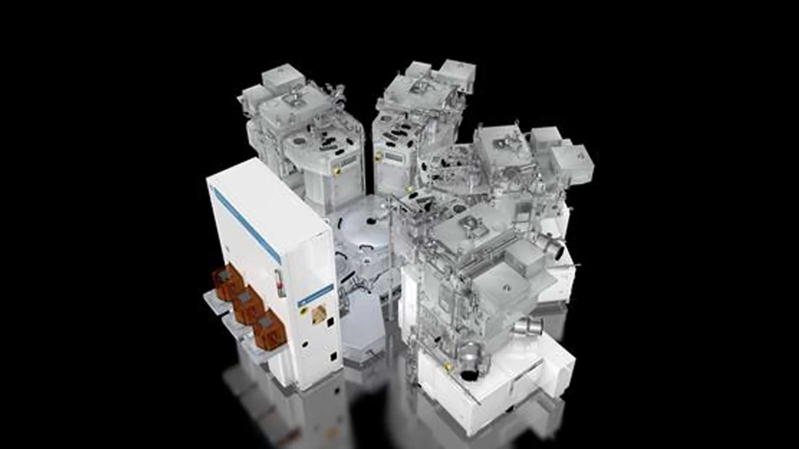
Silicon Valley-based Applied Materials, a leader in making tools for chip manufacturing, recently unveiled a breakthrough lithography technology which will reduce the cost, complexity, and environmental impact of advanced chipmaking.
Lithography is essentially the process of projecting a blueprint of the pattern onto a silicon wafer. The system uses light to focus the pattern onto the wafer. Once it is printed, the process is repeated dozens of times per wafer. However, to print the smallest of features which is even outside the limit of what light can do, tools like Extreme Ultraviolet (EUV) lithography are used.
Applied Materials’ Centura Sculpta patterning system and its new pattern-shaping technology will enable chipmakers to print a single EUV pattern, following which they can use the Sculpta system to elongate the shapes in any direction, reducing the space between features and increasing pattern density.
The single patterning system will save water and energy, and consequently, the cost of wafer production. This technology will save the capital cost of approximately $250 million per 100K wafer starts per month of production capacity.
This is in contrast to the commonly used EUV double patterning, which involves splitting a high-density pattern in half and producing two masks that adhere to the EUV resolution limits. This approach adds complexity to the design and pattern production, making it an expensive proposition for companies.
Furthermore, utilising a single patterning system reduces the number of EUV lithography steps, compared to the double patterning process. “The new Sculpta system is a great example of how advances in materials engineering can complement EUV lithography to help chipmakers optimise chip area and cost while also tackling the growing economic and environmental challenges of advanced chipmaking,” said Dr Prabu Raja, senior vice president and general manager of the Semiconductor Products Group at Applied Materials.
The Dutch multinational corporation ASML holds a monopoly on the fabrication of EUV lithography due to its exploitation of photolithography to an extreme level. A competition however seemed eminent. There were talks that perhaps China has cracked the code for lithography, with the US blocking all sales of lithography equipment to China. And now, with Applied Materials making a leapfrog into it, it does look like the market for lithography tools will finally see a cut-throat competition, which will ultimately benefit the semiconductor industry.
- Amazon Warns Engineers Against AI Productivity Traps in Latest Memo
- Gnani AI Launches Prisma v3.0 Speech Recognition Model for 10 Languages
- Venttup Raises $3 Million To Expand Precision Manufacturing
- Articul8 Launches Bivia To Help Enterprise AI Agents Make Decisions
- NVIDIA Launches Open-Weight Transcription Model for 40 Languages
- Sarvam AI Rolls Out Indus Cowork to 2,500 Maharashtra Govt Officials