
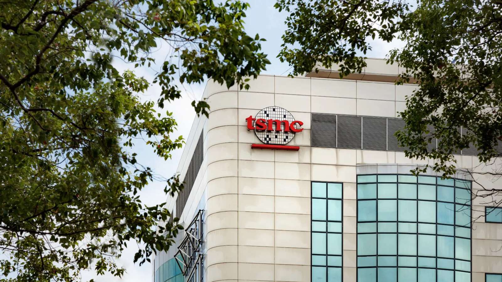
Sony Semiconductor Solutions and TSMC have signed a preliminary agreement to form a strategic partnership to develop and manufacture next-generation image sensors. The companies said they plan to establish a joint venture at Sony’s new fabrication facility in Kumamoto prefecture, Japan.
Under the proposed structure, Sony will remain the majority and controlling shareholder in the joint venture. The companies said the partnership will combine Sony’s image sensor design expertise with TSMC’s semiconductor manufacturing and process technologies.
Shinji Sashida, President and CEO of Sony Semiconductor Solutions Corporation, said that Sony plans to strengthen its operations by developing higher-value products and technologies.
They also plan to expand image sensor applications in physical AI areas such as automotive and robotics.
The companies signed a non-binding MoU for the partnership. They are now discussing possible investments for the joint venture, along with Sony’s additional capital investment in its existing Nagasaki plant. The companies said they will phase out these investments based on market demand and support from the Japanese government.
TSMC Senior VP and Deputy Co-COO, Kevin Zhang, said Sony has been TSMC’s long-term partner in the CMOS image sensor business. He added that the agreement marks a key step in advancing sensing technologies for the AI era.
The companies said the joint venture still depends on signing a final binding agreement and meeting customary closing conditions.
Recently, TSMC introduced its A13 process technology to meet rising demand for AI, high-performance computing, and mobile applications. But the new node builds on A14’s process and will enter production only in 2029, one year after A14.
Moreover, on April 28 and 29, the company sold all its shares in Arm Holdings, primarily owned by the Japanese conglomerate SoftBank Group, according to a company filing accessed by AIM.
- OpenAI Introduces ChatGPT Wallet for Agent-Led Payments
- ReNew Pledges ₹80,000 Cr for Green Data Centre to Fuel India’s AI Push
- Mars Opens Hyderabad GCC With Genpact to Expand Digital, AI Capabilities
- Shield AI Opens Bengaluru Engineering Office to Build Defence Autonomy Software
- Adobe, Google Expand AI Partnership Across Creative and Productivity Tools
- Google Launches Gemini 4 Hydrogen for Faster Coding and AI Workflows