Key takeaways
- ASML collaborates with TSMC, Samsung, and Intel to advance High NA EUV lithography for semiconductor manufacturing.
- Samsung aims to implement High NA technology in DRAM production by 2028, while Intel has already adopted it for select layers.
- TSMC plans to use High NA technology for high-volume manufacturing from 2030, enhancing production capabilities.
- An industry initiative led by ASML and TSMC seeks to transition to 12-inch photomasks by 2031 to improve productivity.
- The shift to larger masks is expected to reduce chipmaking costs and enhance the utilisation of High NA EUV technology.
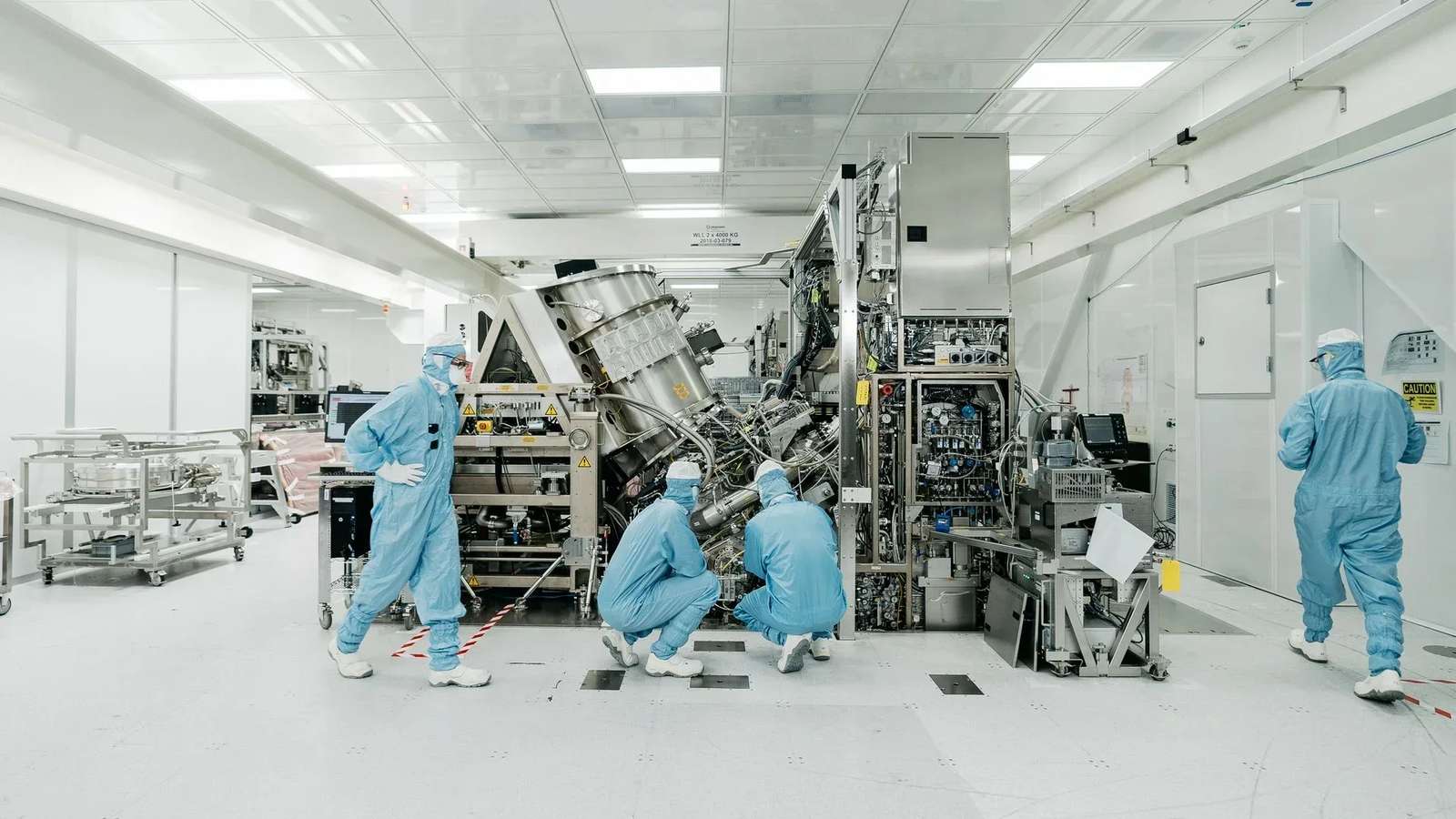
TSMC, Samsung Electronics, and Intel Foundry are advancing High Numerical Aperture (High NA) EUV lithography for semiconductor manufacturing, with each company at a different stage of adoption.
The companies announced the developments in partnership with ASML at industry events focused on EUV technology and photomasks.
TSMC plans to use ASML’s High NA technology in high-volume manufacturing for advanced nodes from 2030. Samsung plans to introduce the technology into future DRAM high-volume manufacturing by 2028. Intel already uses High NA for selected layers in high-volume production.
ASML and TSMC have formed an industry initiative to shift from the current 6-inch photomask format to 12-inch masks. The initiative targets a 12-inch mask pilot line by 2031. It aims to support full lithography system readiness for advanced-node production by 2033.
The companies expect larger masks to increase fab productivity and lower chipmaking costs. They also expect the transition to remove stitching constraints. This would allow chipmakers to use more of High NA EUV’s capabilities.
TSMC Chairman and CEO CC Wei said collaboration across the semiconductor supply chain would help address manufacturing challenges. “We have always believed that when the industry works together to solve complex problems, we unlock possibilities that no single company could achieve alone,” he said in a statement.
Samsung will also join the industry initiative for 12-inch photomask technology. The company will work with industry partners on mask technologies and supporting infrastructure.
ASML CEO Christophe Fouquet said High NA adoption will progress from existing 6-inch masks towards larger formats.
TSMC expects demand for High NA EUV to increase as semiconductor nodes advance. It said more layers will require the technology because AI applications use increasingly complex transistor architectures.
Samsung plans to introduce ASML’s High NA EUV technology into future DRAM high-volume manufacturing by 2028. The company expects improved resolution to support process simplification and greater efficiency.
Samsung CEO Jun Young-Hyun said the company wants to strengthen its position in advanced memory and foundry manufacturing. “By further strengthening our collaboration with ASML, we are helping lay the foundation for the next generation of AI and semiconductor innovation,” he said.
Intel has already processed more than 1 million wafers using High NA across certification, research, development, and volume production. The technology is being used on selected layers of Intel Core Ultra Series 3 processors.
Intel said its 18A products using High NA on selected layers meet or exceed comparable layers made with its NXE EUV platform. The company also supports High NA use with current 6-inch masks through floor planning and stitching solutions.
Naga Chandrasekaran, Executive VP and Co-general Manager of Intel Foundry, said the company is focused on enabling High NA with existing masks while preparing for the larger format. “Intel Foundry is focused on near-term enablement of High NA on 6-inch masks with or without stitching,” he said.
The three chipmakers therefore represent different stages in the industry’s High NA transition. Intel has moved into production, Samsung has set a 2028 DRAM target, and TSMC has set a 2030 advanced-node target. In addition, the companies are also working towards a common 12-inch mask ecosystem.
Spotted an error? Tell our editors. Read our editorial standards and corrections.